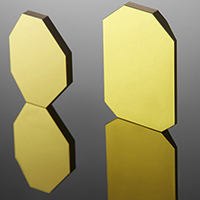
Silicon Scanning Mirrors:SI-SM-355-10-X
Number:SI-SM-355-10-X
Silicon scanning mirrors have the advantages of light weight, small size, good thermal stability, and high mechanical strength. Applied to lasers, telescopes, microscopes, scanners, etc. Accurate optical control and image processing can be achieved by controlling parameters such as the direction and intensity of reflected light. Galvanometer scanning is the process of first incident the laser beam generated by the laser emission device onto the X-axis galvanometer, then reflecting it onto the Y-axis galvanometer. After secondary reflection by the Y-axis galvanometer, it can be projected onto the working plane, forming a scanning point. Then, the beam deflector composed of X and Y scanning heads is driven by a galvanometer motor to deflect the laser beam within the predetermined scanning range, so that the laser focal point with a certain power density leaves a permanent mark on the marking material, completing the scanning of the image. Each beam deflector has a specially designed reflector lens (coated with different optical films to reflect laser of different wavelengths), and the different deflection methods of the two lenses can enable the laser to scan different patterns and print different models.
Please leave a message or inquire about the price online to ensure a satisfactory price for you.
All products are provided with invoices, with a tax point of 13.
The product undergoes multiple inspections before being stored, and the quality is guaranteed. Please use it with confidence.
Spot products, shipped within 48 hours. For non stock or customized products, please consult.
International order logistics include DHL, FedEx, TNT, and EMS
When receiving the product, please ensure the integrity of the product packaging box first. If there is serious damage to the appearance, please refuse and contact us, and we will handle it for you as soon as possible.
Optical products are special items and cannot be returned or exchanged unless there is a quality issue with the product itself
If you need customization or bulk production, please contact us online and we will offer you a discounted price.
| Incident Beam Dia | Dim(mm) | X/Y Type | Wavelength | Coating | Compare | |
|---|---|---|---|---|---|---|
| Screen | Screen | Screen | Screen | Screen | ||
| More+ Less | 10 | 18.3*13*2 | X | 355nm | Dielectric | |

Silicon Scanning Mirrors:SI-SM-355-10-X Number:SI-SM-355-10-X
Incident Beam Dia:10
Dim(mm):18.3*13*2
X/Y Type:X
Wavelength:355nm
Substrate Material:Silicon(Si)
Length Tolerance(mm):+0.0/-0.1
Width Tolerance(mm):+0.0/-0.1
Thk Tolerance(mm):+0.0/-0.05
Surface Quality:60-40
Surface Accuracy:λ/2
Coating:Dielectric
Clear Aperture:90%
|
||||||
| More+ Less | 10 | 23.2*16*2 | Y | 355nm | Dielectric | |

Silicon Scanning Mirrors:SI-SM-355-10-Y Number:SI-SM-355-10-Y
Incident Beam Dia:10
Dim(mm):23.2*16*2
X/Y Type:Y
Wavelength:355nm
Substrate Material:Silicon(Si)
Length Tolerance(mm):+0.0/-0.1
Width Tolerance(mm):+0.0/-0.1
Thk Tolerance(mm):+0.0/-0.05
Surface Quality:60-40
Surface Accuracy:λ/2
Coating:Dielectric
Clear Aperture:90%
|
||||||
| More+ Less | 12 | 21*16.8*2 | X | 355nm | Dielectric | |

Silicon Scanning Mirrors:SI-SM-355-12-X Number:SI-SM-355-12-X
Incident Beam Dia:12
Dim(mm):21*16.8*2
X/Y Type:X
Wavelength:355nm
Substrate Material:Silicon(Si)
Length Tolerance(mm):+0.0/-0.1
Width Tolerance(mm):+0.0/-0.1
Thk Tolerance(mm):+0.0/-0.05
Surface Quality:60-40
Surface Accuracy:λ/2
Coating:Dielectric
Clear Aperture:90%
|
||||||
| More+ Less | 12 | 26*17*2 | Y | 355nm | Dielectric | |

Silicon Scanning Mirrors:SI-SM-355-12-Y Number:SI-SM-355-12-Y
Incident Beam Dia:12
Dim(mm):26*17*2
X/Y Type:Y
Wavelength:355nm
Substrate Material:Silicon(Si)
Length Tolerance(mm):+0.0/-0.1
Width Tolerance(mm):+0.0/-0.1
Thk Tolerance(mm):+0.0/-0.05
Surface Quality:60-40
Surface Accuracy:λ/2
Coating:Dielectric
Clear Aperture:90%
|
||||||
| More+ Less | 14 | 26*16.5*3 | X | 355nm | Dielectric | |

Silicon Scanning Mirrors:SI-SM-355-14-X Number:SI-SM-355-14-X
Incident Beam Dia:14
Dim(mm):26*16.5*3
X/Y Type:X
Wavelength:355nm
Substrate Material:Silicon(Si)
Length Tolerance(mm):+0.0/-0.1
Width Tolerance(mm):+0.0/-0.1
Thk Tolerance(mm):+0.0/-0.05
Surface Quality:60-40
Surface Accuracy:λ/2
Coating:Dielectric
Clear Aperture:90%
|
||||||
| More+ Less | 14 | 31*21.5*3 | Y | 355nm | Dielectric | |

Silicon Scanning Mirrors:SI-SM-355-14-Y Number:SI-SM-355-14-Y
Incident Beam Dia:14
Dim(mm):31*21.5*3
X/Y Type:Y
Wavelength:355nm
Substrate Material:Silicon(Si)
Length Tolerance(mm):+0.0/-0.1
Width Tolerance(mm):+0.0/-0.1
Thk Tolerance(mm):+0.0/-0.05
Surface Quality:60-40
Surface Accuracy:λ/2
Coating:Dielectric
Clear Aperture:90%
|
||||||
| More+ Less | 15 | 28*17*2.5 | X | 355nm | Dielectric | |

Silicon Scanning Mirrors:SI-SM-355-15-X Number:SI-SM-355-15-X
Incident Beam Dia:15
Dim(mm):28*17*2.5
X/Y Type:X
Wavelength:355nm
Substrate Material:Silicon(Si)
Length Tolerance(mm):+0.0/-0.1
Width Tolerance(mm):+0.0/-0.1
Thk Tolerance(mm):+0.0/-0.05
Surface Quality:60-40
Surface Accuracy:λ/2
Coating:Dielectric
Clear Aperture:90%
|
||||||
| More+ Less | 15 | 33.5*22*2.5 | Y | 355nm | Dielectric | |

Silicon Scanning Mirrors:SI-SM-355-15-Y Number:SI-SM-355-15-Y
Incident Beam Dia:15
Dim(mm):33.5*22*2.5
X/Y Type:Y
Wavelength:355nm
Substrate Material:Silicon(Si)
Length Tolerance(mm):+0.0/-0.1
Width Tolerance(mm):+0.0/-0.1
Thk Tolerance(mm):+0.0/-0.05
Surface Quality:60-40
Surface Accuracy:λ/2
Coating:Dielectric
Clear Aperture:90%
|
||||||
| More+ Less | 20 | 37*25.5*3 | X | 355nm | Dielectric | |

Silicon Scanning Mirrors:SI-SM-355-20-X Number:SI-SM-355-20-X
Incident Beam Dia:20
Dim(mm):37*25.5*3
X/Y Type:X
Wavelength:355nm
Substrate Material:Silicon(Si)
Length Tolerance(mm):+0.0/-0.1
Width Tolerance(mm):+0.0/-0.1
Thk Tolerance(mm):+0.0/-0.05
Surface Quality:60-40
Surface Accuracy:λ/2
Coating:Dielectric
Clear Aperture:90%
|
||||||
| More+ Less | 20 | 47*31*3 | Y | 355nm | Dielectric | |

Silicon Scanning Mirrors:SI-SM-355-20-Y Number:SI-SM-355-20-Y
Incident Beam Dia:20
Dim(mm):47*31*3
X/Y Type:Y
Wavelength:355nm
Substrate Material:Silicon(Si)
Length Tolerance(mm):+0.0/-0.1
Width Tolerance(mm):+0.0/-0.1
Thk Tolerance(mm):+0.0/-0.05
Surface Quality:60-40
Surface Accuracy:λ/2
Coating:Dielectric
Clear Aperture:90%
|
||||||
| Material Data | |
| Optical Propertie | |
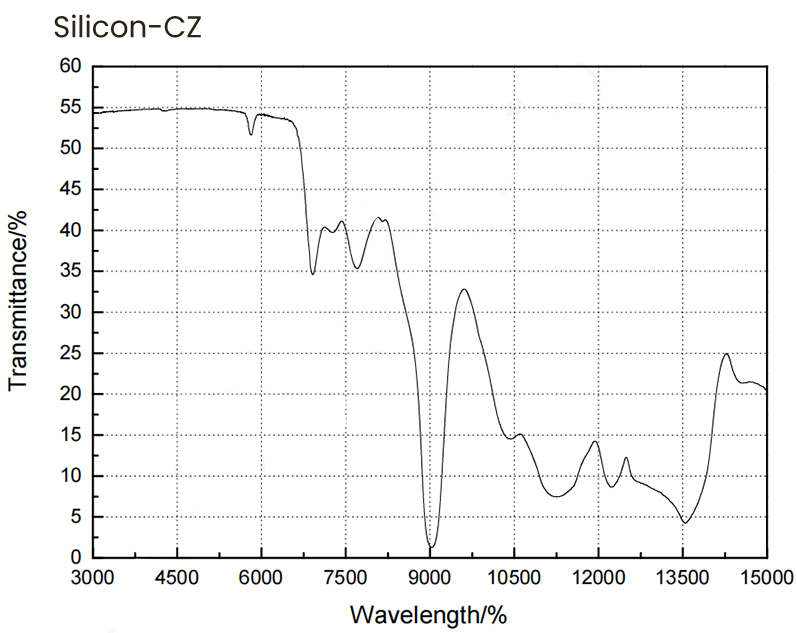
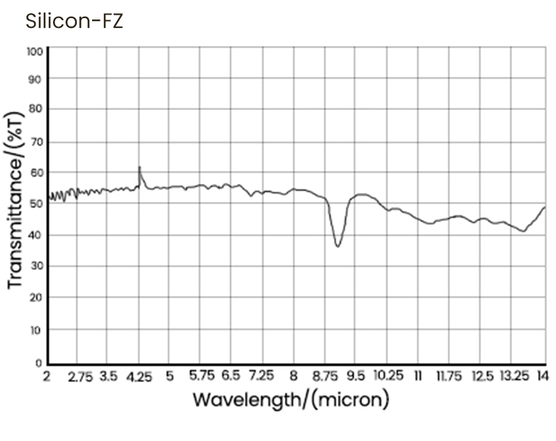
| Transmission Range | 1.2-15μm |
| Refractive Index | 3.41776%@10μm |
| Reflection Loss | 46.1%@10μm |
| Structure | Single crystal,synthetic |
| Cleavage Planes | <111> |
| Physical Properties | |
| Density [g/cm3] | 2.33 |
| Melting Point [℃] | 1414 |
| Thermal Conductivity [W/(m×K)] | 163 @ 313K |
| Thermal Expansion [10-6/K] | 2.6 @ 293K |
| Knoop Hardness [kg/mm2] | 1100 |
| Specific Heat Capacity [J/(kg×K)] | 712.8 |
| Dielectric Constant | 13 @f= 9.37GHz |
| Young's Modulus (E) [GPa] | 130.91 |
| Shear Modulus(G) [GPa] | 79.92 |
| Bulk Modulus(K) [GPa] | 101.97 |
| Poisson Coefficient | 0.266 |
| Chemical Properties | |
| Solubility / g/L | None |
| Molecular Weight / g/mol | 28.09 |
Hot Products
 Domestic free shipping
 Inspection and delivery
 product research
 Professional quality
 Complete category